#Stabilizing monolayer nitrides with silicon
“#Stabilizing monolayer nitrides with silicon”

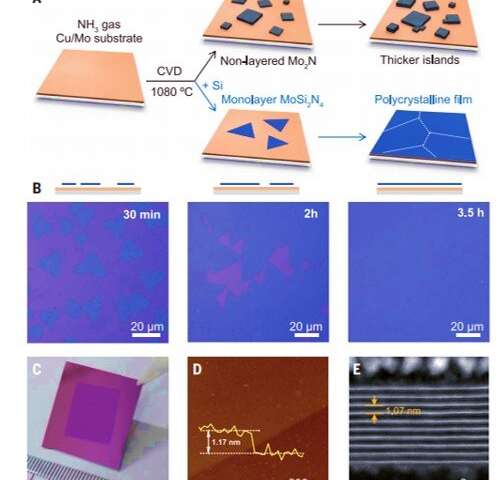
In a new report published in Science, Yi-Lun Hong and a group of research scientists in materials science, engineering, and advanced technology in China and the U.K. investigated two-dimensional (2-D) materials to discover new phenomena and unusual properties. The team introduced elemental silicon during chemical vapor deposition-based growth of molybdenum nitride to passivate its surface and develop centimeter-scale, monolayer nitride films with silicon such as MoSi2N4. They built the monolayer film with seven atomic layers in the order of nitrogen-silicon-nitrogen-molybdenum-nitrogen-silicon-nitrogen (N-Si-N-Mo-N-Si-N), and the resulting material showed semiconducting behavior and excellent stability under ambient conditions. Using density functional theory (DFT) calculations, the scientists predicted a large family of such monolayer structured 2-D materials to exist with useful applications as semiconductors, metals and magnetic half-metals.
Two-dimensional materials
Two-dimensional materials have attractive properties that are suited for a variety of technical applications. Of these, transition metal carbides and nitrides (TMCs and TMNs) can form a large family of non-layered materials to combine properties of ceramics and metals. The MAX phase, where M stands for an early transition metal, A is an A-group element such as aluminum or silicon and X is carbon, nitrogen or both, forms the basis for monolayer MXenes. Such monolayer films can be selectively synthesized by etching the A-element layer. These materials have a hydrophilic (water-loving) surface and high electrical conductivity with promising applications including energy storage, sensors and catalysis. Scientists have recently developed a chemical vapor deposition (CVD) method to grow high-quality, nonlayered 2-D TMC and TMN crystals with diverse structures. But the surface energy constraints caused the nonlayered materials to grow as islands instead of layers. In this work, Hong et al. therefore grew 2-D molybdenum nitride and the MoSi2N4 compound using chemical vapor deposition.

Developing and characterizing the newly formed 2-D materials
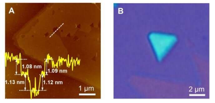
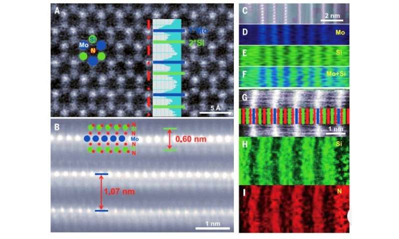
During the experiments, the scientists used a copper/molybdenum (Cu/Mo) bilayer as the substrate and ammonia (NH3) gas as the source of nitrogen. When they introduced elemental silicon to the experimental setup, the growth of the substrate markedly changed to form a uniform polycrystalline film. The team determined the thickness of the material surface using atomic force microscopy (AFM) and noted the surface growth process to be robust. Typically, the addition of an element to a growing 2-D material can only cause doping without changing the crystal structure of the matrix. But in this instance, adding silicon led to a new monolayered compound instead of simply doping the substrate. Hong et al. identified the crystal structure of the newly formed 2-D material using advanced transmission electron microscopy (TEM) and tested its surface elements using energy dispersive x-ray spectroscopy (EDS), electron energy-loss spectroscopy (EELS) and X-ray photoelectron spectroscopy (XPS).

Confirming the MoSi2N4 formula and highlighting the material properties.
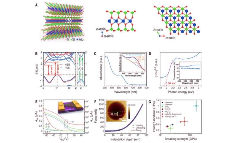
Since it was difficult to image the exact positions of nitrogen atoms using transmission electron microscopy, the team performed density functional theory (DFT) calculations of the compound to reveal its structural formula. The process confirmed the presence of a van der Waals (vdW) layered 2-D material containing the MoSi2N4 formula. Then using molecular dynamics calculations, they observed the structure to be dynamically and thermodynamically stable – while Raman spectra indicated high crystal quality of the MoSi2N4 structure. Using DFT calculations again, Hong et al noted the MoSi2N4 monolayer to maintain semiconductor properties (optical and electrical properties) alongside a carrier mobility that relied on the elastic modulus of the material.

To study the optical properties of the monolayer MoSi2N4 film, Hu et al. transferred it onto a sapphire substrate and measured its bandgap, where the semiconducting monolayer maintained a high optical transmittance comparable to graphene. To test the electrical transport properties of the materials, Hong et al. fabricated back-gated field-effect transistor devices to observe typical semiconductor behavior. The scientists then measured the mechanical properties of the monolayer film using nanoindentation to highlight the elastic behavior of the membrane. The newly formed material showed long-term stability for handling, storage, and processing under ambient conditions without a protective environment in contrast to other materials.

Creating a broad class of 2-D van der Waals (vdW) layered materials
Hong et al. showed how diverse transition metal elements could potentially replace the corresponding elements in MoSi2N4 based on additional DFT calculations to create a broad class of 2-D van der Waal layered materials with similar crystal structure. In this instance, they represented the materials with the general formula of MA2Z4, where M represented an early transition metal, A was silicon or Germanium and Z stood for nitrogen, phosphorous or arsenic. The elemental diversity in MA2Z4, allowed wide tunability of their bandgap and magnetic properties with applications in optoelectronics, electronics and spintronics. Using such materials, the scientists will be able to investigate hitherto unknown exciting properties and applications that exist within layered materials. In this way, the chemical vapor deposition method described here will pave the way to synthesize diverse materials in 2-D and monolayer forms.
More information:
Hong Y. et al. Chemical vapor deposition of layered two-dimensional MoSi2N4 materials, Science Advances, 10.1126/science.abb7023
A. K. Geim et al. The rise of graphene, Nature Materials (2007). DOI: 10.1038/nmat1849
Wang Q. H. et al. Electronics and optoelectronics of two-dimensional transition metal dichalcogenides, Nature Nanotechnology, 10.1038/nnano.2012.205
© 2020 Science X Network
Stabilizing monolayer nitrides with silicon (2020, August 14)
retrieved 14 August 2020
from https://phys.org/news/2020-08-stabilizing-monolayer-nitrides-silicon.html
This document is subject to copyright. Apart from any fair dealing for the purpose of private study or research, no
part may be reproduced without the written permission. The content is provided for information purposes only.
If you want to read more Like this articles, you can visit our Science category.
if you want to watch Movies or Tv Shows go to Dizi.BuradaBiliyorum.Com for forums sites go to Forum.BuradaBiliyorum.Com


