#Angstrom multilayer metrology by combining spectral measurements and machine learning

“#Angstrom multilayer metrology by combining spectral measurements and machine learning”

With the recent explosive demand for data storage, ranging from data centers to various smart and connected devices, the need for higher-capacity and more compact memory devices is constantly increasing. As a result, semiconductor devices are now moving from 2-D to 3-D. The 3-D-NAND flash memory is the most commercially successful 3-D semiconductor device today, and its demand for supporting our data-driven world is now growing exponentially.
The scaling law for 3-D devices is achieved by stacking more and more semiconductor layers, well above 100 layers, in a more reliable way. As each layer thickness corresponds to the effective channel length, accurate characterization and control of layer-by-layer thickness is critical. To date, unfortunately, non-destructive, accurate measurement of each layer thickness of such hundreds-layers structure has not been possible, which sets a serious bottleneck in the future scaling of 3-D devices.
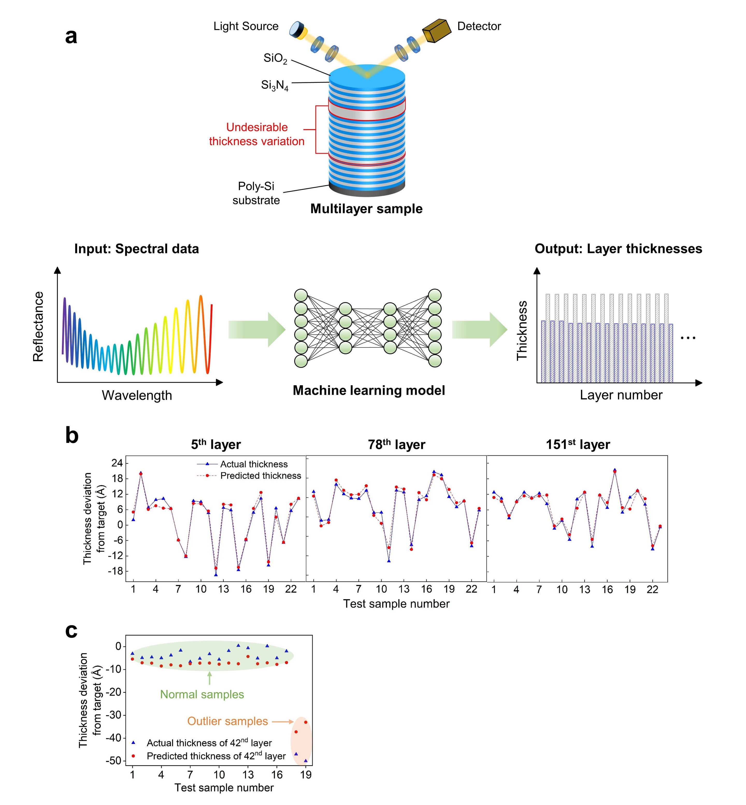
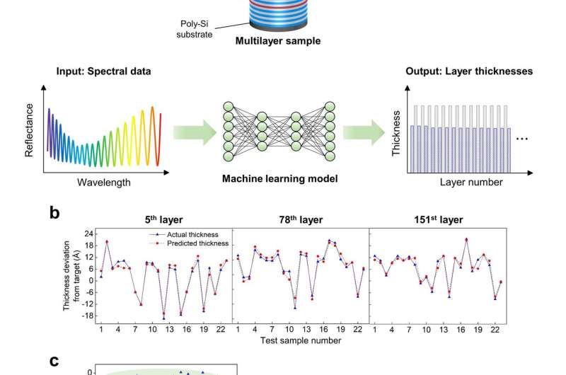
In a new paper published in Light: Advanced Manufacturing, a team of engineers from Korea Advanced Institute of Science and Technology (KAIST) and Samsung Electronics Co. Ltd., led by Professor Jungwon Kim of KAIST, South Korea, has developed a non-destructive thickness characterization method by combining optical spectral measurements and machine learning. By exploiting the structural similarity between semiconductor multilayer stacks and dielectric multilayer mirrors, spectroscopic optical measurements, including ellipsometric and reflectance measurements, are employed. Machine learning is then used to extract the correlation between spectroscopic measurement data and multilayer thickness. For more than 200 layers of oxide and nitride multilayer stack, the thickness of each layer over the entire stack could be determined with an average of approximately 1.6 Å root-mean-square error.
In addition to the accurate determination of the multilayer thickness under normal fabrication conditions, which is helpful for controlling etching and deposition processes, the research team developed another machine learning model that can detect outliers when layer thicknesses significantly vary from the design target. It used a large number of simulated spectral data for more effective and economical training, and could successfully detect the faulty devices and the exact erroneous layer location in the device.
“The machine learning approach is useful for eliminating measurement-related issues,” said Hyunsoo Kwak, a doctoral student at KAIST and first author of the study. “By using noise-injected spectral data as input to the machine learning algorithm, we can eliminate various errors from measurement instruments and changes in material properties under different fabrication conditions,” he added.
“This method can be readily applied for the total inspection of various 3-D semiconductor devices,” said Professor Kim, “which is exemplified by the fact that all the data used in this work were obtained in commercial 3-D NAND manufacturing lines of Samsung Electronics.”
Producing materials to help break the electronics scaling limit
Hyunsoo Kwak et al, Non-destructive thickness characterisation of 3D multilayer semiconductor devices using optical spectral measurements and machine learning, Light: Advanced Manufacturing (2021). DOI: 10.37188/lam.2021.001
Citation:
Angstrom multilayer metrology by combining spectral measurements and machine learning (2021, January 21)
retrieved 22 January 2021
from https://phys.org/news/2021-01-angstrom-multilayer-metrology-combining-spectral.html
This document is subject to copyright. Apart from any fair dealing for the purpose of private study or research, no
part may be reproduced without the written permission. The content is provided for information purposes only.
If you liked the article, do not forget to share it with your friends. Follow us on Google News too, click on the star and choose us from your favorites.
For forums sites go to Forum.BuradaBiliyorum.Com
If you want to read more Like this articles, you can visit our Science category.


