#Goodbye, DonGlees! & Misaki no Mayoiga Compete at Annecy International Animation Film Festival

Table of Contents
“Goodbye, DonGlees! & Misaki no Mayoiga Compete at Annecy International Animation Film Festival”
The Annecy International Animation Film Festival announced ten nominees for this year’s feature film competition category on May 2, including two Japanese anime films – Goodbye, DonGlees! directed by Atsuko Ishizuka (A Place Further than the Universe) and Misaki no Mayoiga (The House of the Lost on the Cape) by Shinya Kawatsura (Non Non Biyori). 2022’s Annecy Festival will run from June 13 to 18.
#OfficialSelection ????️
It’s time to reveal the final part of the Official Selection, the most anticipated Feature Films… ???? A selection of 10 surprising and diverse films that testify to the vibrancy of #animation film! pic.twitter.com/WPy5gQVWYs
— Annecy Festival (@annecyfestival) May 2, 2022
Feature Films Category Nominees:
- “Charlotte” by Eric Warin, Tahir Rana – Belgium, Canada, France
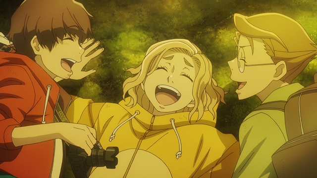
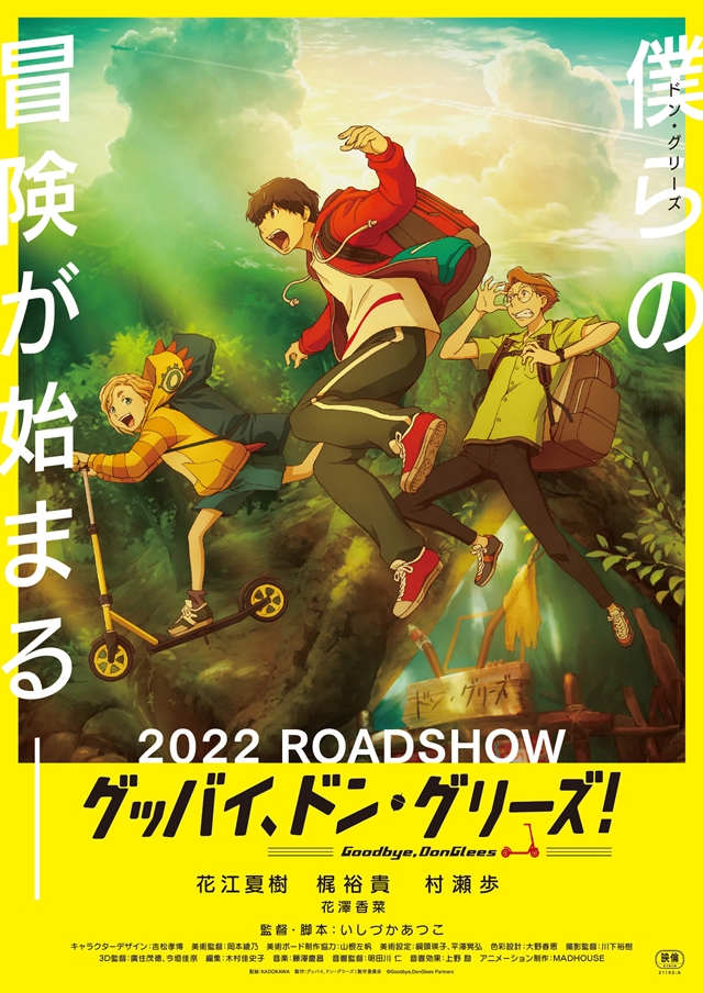
- “Goodbye, DonGlees!” by Atsuko Ishizuka – Japan
- “Interdit aux chiens et aux Italiens” by Alain Ughetto – France, Italy
- “The Island” by Anca Damian – Romania, France, Belgium
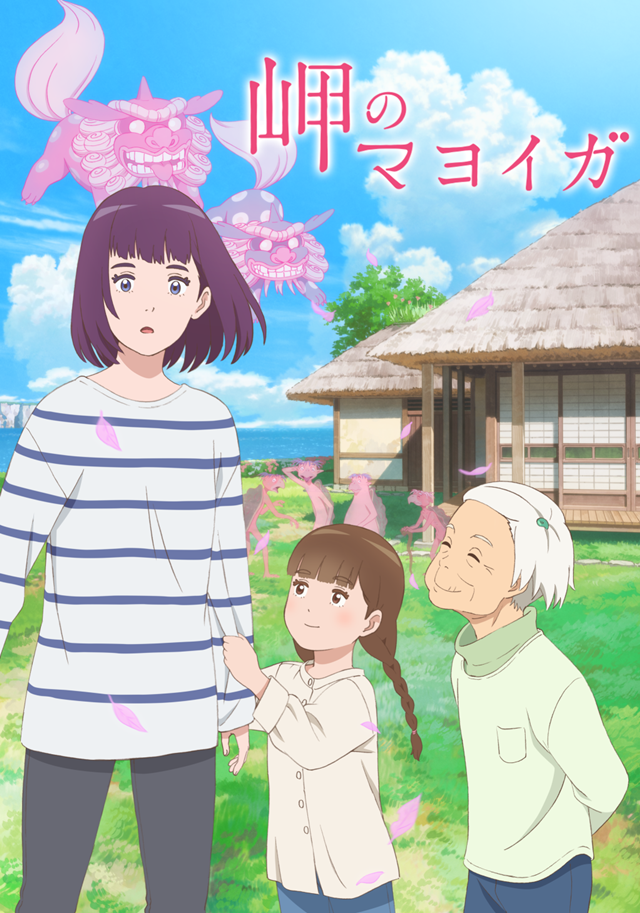
- “The House of the Lost on the Cape (Misaki no Mayoiga)” by Shinya Kawatsura – Japan
- “My Love Affair with Marriage” by Signe Baumane – USA, Latvia, Luxembourg
- “Nayola” by José Miguel Ribeiro – Portugal, Belgium, Netherlands, France
- “Little Nicholas – Happy as Can Be” by Amandine Fredon, Benjamin Massoubre – France, Luxembourg
- “Blind Willows, Sleeping Woman” by Pierre Foldes – Canada, France, Luxembourg
- “Unicorn Wars” by Alberto Vazquez – Spain, France
Goodbye, DonGlees, based on director Ishizuka’s own original screenplay, was released in 217 Japanese theaters on February 18, 2022, and didn’t rank in the top 10 in its opening weekend.
Trailer:
Poster visual:
Misaki no Mayoiga, based on Sachiko Kashiwaba’s fantasy novel of the same name published by Kodanhsa in 2015, was released in Japan on August 27, 2021, and also didn’t appear in the box office top 10 in its opening weekend. Later, the 76th Mainichi Film Awards chose it as the Best Animation Film of 2021.
RELATED: The House of the Lost on the Cape Wins The 76th Mainichi Film Award’s Best Animation Film
Trailer:
Poster visual:
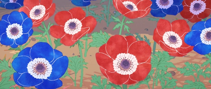
Meanwhile, the festival’s official site also revealed Naoko Yamada‘s (Tamako Market, A Silent Voice) new short film Garden of Remembrance in its Work in Progress section. SCIENCE SARU, Eunyoung CHOI, and AVEX PICTURES are named as production companies. The 15-minute short is described as below:
An untidy room. Empty beer tins, empty wine bottles, a half-empty glass of whisky… A girl is getting up absent-mindedly and starts preparing herself. YOUR morning starts. Lazy and hard-to-wake-up YOU. The emoticon is ME watching over YOU. I play tricks on YOU, while YOU are playing the guitar and drinking. One day, in town, YOU walk past THE CHILDHOOD FRIEND who is buying an Anemone I liked, and remembering that I liked them, YOU rush out to buy them. THE CHILDHOOD FRIEND displays the Anemone with care. One day, years after I died, YOU hear noise from the closet. Opened, YOU see MY garden right in front of YOU. Overflowing emotions of ME and YOU. When exiting from the room with memories, a picture of the Anemone that YOU painted is displayed in YOUR new room.
Source: The Annecy International Animation Film Festival official website
©Sachiko Kashiwaba, KODANSHA/2021″Misaki no Mayoiga” Production Committee
©Goodbye,DonGlees Partners
![]()
If you liked the article, do not forget to share it with your friends. Follow us on Google News too, click on the star and choose us from your favorites.
For forums sites go to Forum.BuradaBiliyorum.Com
If you want to read more anime-manga articles, you can visit our anime-manga category.


