#White graphene exhibits high defect tolerance and elasticity
“#White graphene exhibits high defect tolerance and elasticity”
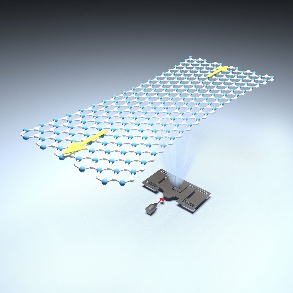
 can be up to 6.2%. Credit: City University of Hong Kong (CityU)")
Because of their unique physical, chemical, electrical and optical properties, two-dimensional (2-D) materials have attracted tremendous attention in the past decades. After revealing the realistic strength and stretchability of graphene, nicknamed “black gold,” researchers from City University of Hong Kong (CityU) have carried forward the success by unveiling the high defect tolerance and elasticity of hexagonal boron nitride (h-BN), another 2-D material known as “white graphene.” This follow-up study will promote future development and applications of strain engineering, piezoelectronics and flexible electronics.
Since British scientists exfoliated single-atom-thick crystallites from bulk graphite in 2004 for the first time, research on 2-D materials has undergone rapid advances. Novel 2-D materials have been discovered, including hexagonal boron nitride (h-BN), the focus of this article, transition metal dichalcogenides (TMDs) such as MoS2, and black phosphorus (BP). Those successfully isolated 2-D materials have different band gaps (from 0 to 6 eV), and range from conductors, semiconductors to insulators, which illustrates their potential in electronic device applications.
The conductivity of a material is determined by energy bands. When there is a small energy gap between the valence band and the conduction band (the band gap value is close to 0), electrons can move freely between the two energy bands, that is a conductor. When the gap between the valence band and the conduction band is large (the band gap value is close to 6), electrons are trapped in the valence band and cannot jump freely, that is an insulator. When the band gap value can be controlled by externally applied electric field, that is a semiconductor.
Sometimes referred as “white graphene,” h-BN shares a similar structure with graphene. The theoretical estimates of its mechanical properties and its thermal stability are also comparable to those of graphene. Due to its ultra-wide band gap of ~6 eV, h-BN can serve in optoelectronics or as a dielectric substrate for graphene or other 2-D materials-based electronics. More importantly, its band gap could be modified via the elastic strain engineering (ESE) approach in which the material band structure can be significantly tuned by lattice straining or distortion.
It is worth mentioning that h-BN can improve the performance of graphene devices. Similar to graphene’s atomic structure, monolayer h-BN has a small lattice mismatch and ultra-flat surface, which can significantly enhance graphene’s carrier density. Carrier density represents the number of carriers that participates in conduction, which is one of the key factors contributing to electrical conductivity. In addition, the ultra-wide band gap makes h-BN an ideal dielectric substrate for graphene and other 2-D material-based electronics. Having no center of symmetry, monolayer h-BN is predicted to exhibit induced piezoelectric potential under mechanical strains.
However, these fascinating properties and applications always require relatively large and uniform deformations. In fact, all materials need to have reliable mechanical properties before they can be used in practical devices.
")
That is why researchers have tried different approaches to explore the mechanical responses of graphene and other 2-D materials under various conditions. Yet, most of the tests use the nanoindentation technique based on atomic force microscopy (AFM), in which the size of the indenter tip limits the testing area of the sample, and the strain is highly non-uniform.
Moreover, research that involves transferring samples of 2-D materials onto a flexible substrate to introduce stretching has faced certain limitations. Due to the weak adhesion between 2-D materials and substrate interface, it is very challenging to apply large strain on the samples of 2-D materials. Hence tensile stretching of large pieces of freestanding monolayer h-BN and the effects of naturally occurring defects on its mechanical robustness remain largely unexplored.
Over the past three years, the research team led by Dr. Lu Yang, Associate Professor of the Department of Mechanical Engineering (MNE) at CityU worked tirelessly with another team from Tsinghua University to develop the world’s very first quantitative in-situ tensile testing technique for free-standing 2-D materials. Recently, they have expanded their research efforts from monolayer graphene to h-BN.
Using the 2-D nanomechanical platform previously developed by the team, the researchers successfully performed quantitative tensile straining on freestanding monolayer h-BN for the first time (see Figure 1). The experiment showed that its fully recoverable elasticity was up to 6.2% and the corresponding 2-D Young’s modulus was about 200 N/m.
Another focus of the research was to explore the effects of h-BN’s naturally occurring defects on structural integrity and mechanical robustness. The team discovered that, monolayer h-BN containing voids of ~100 nm can be even strained up to 5.8% (see Movie/GIF). The atomistic and continuum simulations showed that compared to the imperfections introduced during sample preparation, the elastic limit of h-BN is virtually immune to naturally occurring atomistic defects (such as grain boundaries and vacancies). Those sub-micrometer voids are not detrimental, only reducing the elastic limit of h-BN from ~6.2% to ~5.8%, which demonstrates its high defect tolerance.
“Based on our experimental platform, we managed to investigate the mechanical properties of another important 2-D material. For the first time, we demonstrated the high stiffness and large uniform elastic deformation of monolayer h-BN. The encouraging results not only contribute to the development of h-BN applications in strain engineering, piezoelectronics and flexible electronics, but also propose a new way to improve the performance of 2-D composites and devices. They also provide a powerful tool to explore the mechanical properties of other 2-D materials,” Dr. Lu said.
Their findings were published in Cell Reports Physical Science, an open access journal from Cell Press, titled “Large Elastic Deformation and Defect Tolerance of Hexagonal Boron Nitride Monolayers.”
Ying Han et al. Large Elastic Deformation and Defect Tolerance of Hexagonal Boron Nitride Monolayers, Cell Reports Physical Science (2020). DOI: 10.1016/j.xcrp.2020.100172
Provided by
City University of Hong Kong
Citation:
White graphene exhibits high defect tolerance and elasticity (2020, September 24)
retrieved 24 September 2020
from https://phys.org/news/2020-09-white-graphene-high-defect-tolerance.html
This document is subject to copyright. Apart from any fair dealing for the purpose of private study or research, no
part may be reproduced without the written permission. The content is provided for information purposes only.
For forums sites go to Forum.BuradaBiliyorum.Com
If you want to read more Like this articles, you can visit our Science category.