#Meet the Main Mercs of Combatants Will Be Dispatched! TV Anime

“#Meet the Main Mercs of Combatants Will Be Dispatched! TV Anime”
If you've got a hankering to witness the science fiction genre deliver a whupping to the fantasy genre, then you're in luck, because a new set of character settings and a special promotional illustration have been published for Combatants WIll Be Dispatched! (known in Japan as Sentoin, Hakenshimasu!), an upcoming TV anime based on the series of humorous light novels written by Natsume Akatsuki (KONOSUBA -God's blessing on this wonderful world!) and illustrated by Kakao Lanthanum about an evil mega-corporation that invades an alien planet that looks a lot like a magical fantasy world.
The new character settings include:
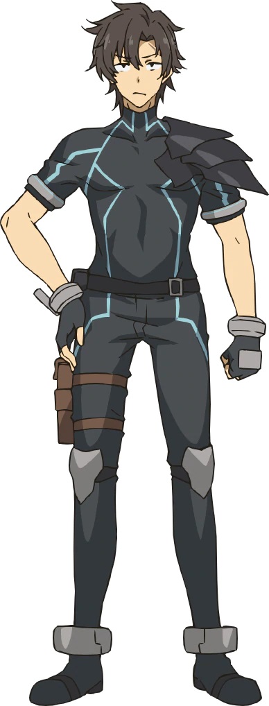
Combat Agent Six (CV: Yūsuke Shirai), the most senior combatant of the Kisaragi Corporation. Although he is extremely capable in battle and has earned a lot of trust from the executives over the years, Combat Agent Six has a rotten personality and his unruly behavior keeps getting him passed over for promotion.

And Alice Kisaragi (CV: Miyu Tomita), an android designed by Kisaragi Corporation. Although she is very pretty and delicate in appearance, Alice sports a high-performance brain and a self-destruct mechanism, and she has an acidic temperment that leads her to insult both enemies and allies alike. Her combat power matches her appearance, i.e. that of an ordinary young lady. Alice hates unscientific things like magic and the occult.

Additionally, a new illustration (above) by original illustrator Kakaou Lanthanum has been published to celebrate the series being adapted into a TV anime.
The original Combatants Will Be Dispatched! light novels are published in Japan by Kadokawa under their Kadokawa Sneaker Bunko imprint, and English language versions are also available from Yen Press, who describe the story of the series as follows:
Always bring a gun to a sword fight! With world domination nearly in their grasp, the Supreme Leaders of the Kisaragi Corporation–an underground criminal group turned evil megacorp–have decided to try their hands at interstellar conquest. A quick dice roll nominates their chief operative, Combat Agent Six, to be the one to explore an alien planet…and the first thing he does when he gets there is change the sacred incantation for a holy ritual to the most embarrassing thing he can think of. But evil deeds are business as usual for Kisaragi operatives, so if Six wants a promotion and a raise, he'll have to work much harder than that! For starters, he'll have to do something about the other group of villains on the planet, who are calling themselves the "Demon Lord's Army" or whatever. After all, this world doesn't need two evil organizations!

Combatants Will Be Dispatched! is directed by Hiroaki Akagi and features animation production by J.C. Staff. The series is scheduled to begin broadcasting in Japan in April of 2021.
Sources:
Ota-suke
Copyright notice: © Natsume Akatsuki, Kakao Lanthanum / KADOKAWA / "Combatants Will Be Dispatched!" Production Committee

—
Paul Chapman is the host of The Greatest Movie EVER! Podcast and GME! Anime Fun Time.
If you liked the article, do not forget to share it with your friends. Follow us on Google News too, click on the star and choose us from your favorites.
For forums sites go to Forum.BuradaBiliyorum.Com
If you want to read more anime-manga articles, you can visit our anime-manga category.


