#Nitride ferroelectric semiconductors for next-generation electronics
“#Nitride ferroelectric semiconductors for next-generation electronics”
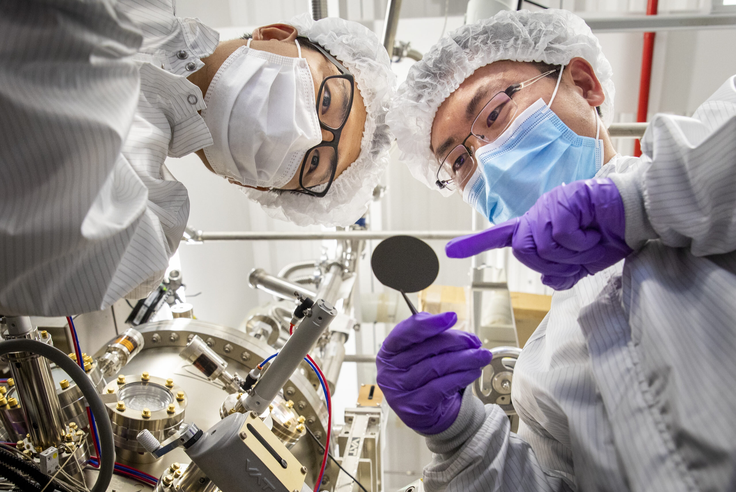
 and Ping Wang (right) check the surface of a single-crystalline ferroelectric ScAlN wafer grown utilizing molecular beam epitaxy. Credit: Robert Coelius")
For the first time, researchers achieved single-crystalline high quality ferroelectric III-V semiconductors that can be integrated into existing platforms for a broad range of ferroelectric, electronic, optoelectronic, and photonic device applications.
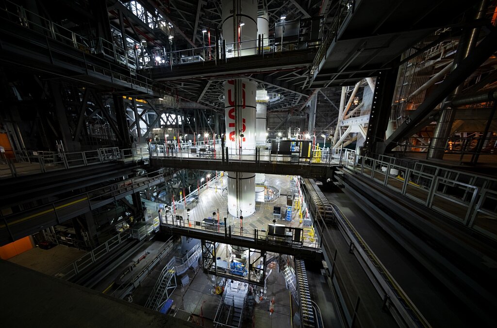
The ferroelectric semiconductor was made using a molecular beam epitaxy (MBE) system, which is already used to manufacture mainstream nitride-based devices.
Their achievement paves the way to a new generation of semiconductors that offer post-Moore’s Law performance with a wide variety of applications.
“From a scientific point of view, we were very excited to work on this,” said Zetian Mi, a professor of Electrical and Computer Engineering who led the research. “We wanted to see if we could create a ferroelectric III-V semiconductor by MBE, which was seen as a big challenge in the community.”
A semiconductor that is ferroelectric allows for the switching of electrical polarization. This quality is particularly promising in microelectronic memory devices for neuromorphic computing and artificial intelligence, where it can result in longer retention times, lower energy costs, higher integration density, and increased robustness in harsh environments.
With its endless possibilities for improving devices with transistors, LEDs, lasers, photovoltaics, and power electronics, ferroelectric semiconductors also have the ability to enhance 5G technology for mobile communications, and is also being explored for use in biological research.
But to be commercially successful, the ferroelectric semiconductor has to be reliable, reproducible, and precisely tuned to the needs of the application.
Mi had been leading research on gallium nitride (GaN) semiconductors for more than a decade. GaN-based semiconductors possess special qualities that allow them to emit light efficiently across the ultraviolet and entire visible spectra and to outperform silicon in high-power, high-frequency, and high-temperature electronic devices and systems.
Nitride semiconductors could truly become the material of the future by adding ferroelectricity to their list of attributes.
In 2019, alloying scandium with aluminum nitride, Mi’s experimental research team demonstrated the epitaxial growth of single-crystalline wurtzite ScAlN, which was theoretically predicted as a ferroelectric material. They were not alone in this exciting discovery, as other researchers began to report the same result.
Almost immediately, funding programs emerged both in the U.S. and abroad to support further research. It became a race to see who could grow this class of semiconductor through a process compatible with mainstream nitride devices, while precisely controlling its electrical polarization.
Research groups have reported some success using a process called sputtered deposition, which does not require the ultra-high vacuum environment of MBE. However, this technique results in polycrystalline materials, which are of much lower quality than materials with a single-phase wurtzite crystal structure.
The breakthrough reported by Mi and his team of postdoctoral researchers Ping Wang and Ding Wang was to create high-quality, controllable and tunable ferroelectric ScAlN semiconductors with a pure wurtzite crystal structure, using MBE processing.
Creating new materials by MBE involves significant trial and error as researchers test different substances to see how they interact under controlled conditions. Individual layers of material may be merely an atom thick, and many variables can impact the outcome. But once the recipe is known, it can be repeated for high-volume manufacturing of semiconductors devices like transistors.
Through their unique process, Mi’s team was able to precisely control both the current leakage in the materials and their electrical polarization. They anticipate being able to scale their devices into the nanometer regime.
The study is titled “Fully epitaxial ferroelectric ScAlN grown by molecular beam epitaxy,” published in Applied Physics Letters.
CMOS-compatible 3-D ferroelectric memory with ultralow power and high speed
Ping Wang et al, Fully epitaxial ferroelectric ScAlN grown by molecular beam epitaxy, Applied Physics Letters (2021). DOI: 10.1063/5.0054539
Citation:
Nitride ferroelectric semiconductors for next-generation electronics (2021, June 11)
retrieved 11 June 2021
from https://techxplore.com/news/2021-06-nitride-ferroelectric-semiconductors-next-generation-electronics.html
This document is subject to copyright. Apart from any fair dealing for the purpose of private study or research, no
part may be reproduced without the written permission. The content is provided for information purposes only.
If you liked the article, do not forget to share it with your friends. Follow us on Google News too, click on the star and choose us from your favorites.
For forums sites go to Forum.BuradaBiliyorum.Com
If you want to read more Like this articles, you can visit our Science category.