#Minimal-interface structures constrained in polycrystalline copper with extremely fine grains
“#Minimal-interface structures constrained in polycrystalline copper with extremely fine grains”
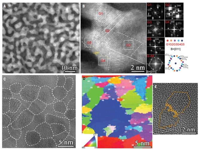
 A typical bright-field TEM image. (B) (Left) A magnified image of a selected area in (A). Dashed lines represent {111} planes and solid lines show CTBs. (Right) Corresponding FFT images of grains (G1, G2, G3, G4, and G5) labeled in the left panel. G-All indicates all grains, with a schematic on the right. (C) A typical high-resolution TEM image. (D) A typical inverse pole figure (IPF) image acquired from a region in (C) from the precession electron diffraction analysis. Numbers indicate misorientation angles of GBs. (E) A typical structural-unit–type boundary as outlined between two tiny grains. Credit: Science, doi: 10.1126/science.abe1267")
Metals with nanoscale crystal grains are super-strong although they do not retain their structure at higher temperatures. As a result, it is challenging to explore their high strength during materials applications. In a new report now published on Science, X. Y. Li and a team of scientists in materials science and engineering at the Chinese Academy of Sciences and Shanghai Jiaotong University in China, found a minimum-interface structure in copper (Cu) with 10-nanometer-sized grains, which they combined with a nanograin crystallographic twinning network to retain high strength at temperatures just below the melting point. The discovery provided a different path to obtain stabilized nanograined metals for metallurgy and materials engineering applications.
Locking in the nanoscale strength
Metals exist as polycrystalline solids that are thermodynamically unstable due to their disordered grain boundaries (GB) and tend to be more stable when grain boundaries are eliminated to ultimately form single crystals. Using experiments and molecular dynamics simulations Li et al. discovered a different type of metastable state for extremely fine-grained polycrystalline pure copper (Cu). For fine-grained polycrystals with a high enough grain boundary density, transformation into a metastable amorphous state is an alternative option to stabilization and is anticipated from a thermodynamic viewpoint. Such amorphous states, however, rarely form for most metallic alloys and pure metals under conventional conditions, therefore it remains to be understood if other metastable structures may be adopted when polycrystalline grains are steadily refined to extremely small scales.
A metastable state at the nanoscale
For instance, when grains of copper (Cu) and nickel (Ni) are refined to a few tens of nanometers in size through plastic deformation, the process can trigger the autonomous grain boundary relaxation into low-energy states with grain boundary dissociations. Nanograined structures may therefore evolve into more stable states by approaching the grain-size extreme. Using experimental and molecular dynamics (MD) simulations, Li et al. discovered a metastable state in polycrystalline pure Cu with grain sizes of a few nanometers, formed by the evolution of grain boundaries into three-dimensional (3-D) minimal interface structures constrained via twin boundary networks.
 A tiny grain of ~2 nm in size. (B) A part of an ideal truncated-octahedron with 1154 atoms (top), rotated by 49° along the [110] axis (lower right). The projected atomic positions on the (001) plane (lower left), are coincident with the TEM image in (A) (where only border atoms are shown in orange). Corner atoms in blurred contrast are circled in (A). (C) A grain containing twins. (D) An ideal truncated-octahedron of 11,817 atoms (top), rotated by 25.5° about the ½011 axis after introducing twins (lower right). Projected atomic positions (bottom left) agree with the TEM image in (C) (where only border atoms in orange and twin boundary atoms in red are shown). Missing corners are indicated by orange arrows in (C). (E) Two grains containing stacking faults (SFs) and twins. (F) Two attached truncated octahedral grains of different sizes with projected atomic positions agreeing with the TEM image in (E). Credit: Science, doi: 10.1126/science.abe1267")
During the experiments, the team used a two-step plastic deformation process of surface mechanical grinding treatment and high-pressure torsion in liquid nitrogen to refine grains of polycrystalline copper with a purity of 99.97 weight percentage at the nanoscale. Using bright-field transmission electron microscopy, Li et al. obtained images of the extremely fine grains, where the specimen appeared as irregular aggregates or chains connected to each other to form continuous networks. The aggregates were made of several individual grains of a few nanometers in size. The tiny crystallites were connected to each other via atomically thin boundaries and the team did not detect amorphous phases or pores.
Characterizing the grains
Li et al. characterized the individual grains of the material by tilting the specimens under high-resolution transmission electron microscopy to resolve their lattice images and identified diverse geometries for many individual grains. The shapes of the grains resembled a truncated octahedron; a favorable option for grains smaller than 10 nanometers. The team determined the thermal stability of as-prepared Cu samples with an average grain-size of 10 nm through isothermal annealing at various temperatures. Li et al. detected more twins in the annealed grains, potentially due to further dissociation of grain boundaries during annealing at elevated temperatures. By elevating the temperatures above 1357 K, the scientists induced melting, at which point all nanograins disappeared.
They then prepared another sample with larger grains for comparison with the same process, but with smaller strain. The observations supported the idea that grain boundary relaxations in polycrystals with smaller grain size will improve stability. Using nanoindentation experiments, they noted unusual stability for the extremely well refined grains in the polycrystalline structure.
 Grain size variations as a function of annealing temperature for three samples with initial average grain sizes of 50 nm, 25 nm, and 10 nm, respectively. Each point of grain size was averaged from >300 grains. (B) A TEM image of the sample with an initial grain size of 10 nm after annealing at 1348 K for 15 min. (C) A high-resolution TEM image of a grain in (B). Red lines indicate twin boundaries. (D) Grain coarsening temperatures (TGC) and strength as a function of grain size in pure Cu. Literature data for Cu samples prepared through various processes are included. Data for amorphous Cu alloys are from referenced literature. Tm, melting point of Cu; tmax, ideal shear strength of Cu. Each grain coarsening temperature was obtained from three independent experiments, and each strength datum was obtained from 10 independent experiments. Exp., experimental; SMGT, surface mechanical grinding treatment; IGC, inert gas condensation; ECAP, equal channel angular pressing; HPT, high-pressure torsion; DPD, dynamic plastic deformation; ED(NT), electrodeposition (nanotwin); CR, cold rolling. Credit: Science, doi: 10.1126/science.abe1267")
Developing an atomistic model
The team then setup an atomistic model to investigate the outstanding stability of the extremely fine Cu grains. To accomplish this, they constructed an extended Kelvin supercell in reference to the Kelvin model, with 16 truncated octahedra-shaped grains of equal size and recognized the fundamental characteristics of grain boundary networks. The team also chose an extended Kelvin polycrystal with an initial grain size of 3.27 nm as a starting structure for simplicity and conducted MD (molecular dynamics) simulations to relax the sample by heating it up at different target temperatures. During molecular dynamic relaxation and subsequent heating, the grain boundaries in the extended Kelvin polycrystal transformed into different structures through varied events.
While some grains shrank and finally disappeared upon heating due to grain boundary migration, the entire grain boundary network did not collapse, instead merging and developing into different forms to topologically resemble the Schwarz D surface (surfaces periodic in three dimensions). According to the MD results, the transformation was thermodynamically driven. Additionally, the polycrystalline structure with Schwarz D interfaces was more stable than Kelvin polycrystals.
 The original Kelvin model of two ideal truncated-octahedra of equal volume (K1 and K2) in 1 by 1 packing (top left). A polycrystal of 16 grains (right) was constructed using a 4 by 4 packing Kelvin model (initial grain size, 6.6 nm). A space-filling 3D CTB network was constructed with a specified lattice orientation for individual grains (see Supplementary Materials). (B) (Left) MD-obtained twin-bounded polycrystalline structure at 0 K, demonstrated by 2 by 2 by 2 supercells where atoms in fcc lattice sites are removed. (Right) GBs resembling the Schwarz D-interface in a 1 by 1 by 1 supercell. (C) A section-view of the Schwarz crystal showing Schwarz D-GBs constrained by CTB networks. (D) The MD-obtained yield stress as a function of temperature. Error bars quantify uncertainty caused by rate effects and thermal fluctuations. Credit: Science, doi: 10.1126/science.abe1267")
The role of the Schwarz D-structure
The Schwarz D structure obtained in this work remained stable at elevated temperatures. Instead of coarsening, grain boundary roughening occurred as the melting point approached; at which point the liquid phase was nucleated heterogeneously at 1321 K, suggesting upper thermal stability to be limited kinetically by grain boundary melting. The team conducted uniaxial tensile-loading tests on the coherent twin boundary (CTB)-constrained Schwarz D structure at various temperatures and strains. They credited the primary mode of observed deformation to twinning and the critical stress corresponding to incipient twinning was temperature dependent.
 upper: MD snapshots of Kelvin supercell at three temperatures as indicated; lower: the evolution of meshed GBs. (B) the Schwarz crystal after cooling down to 1K. Atoms at fcc lattice sites were removed for better visualization effects. (C) upper: MD obtained calorimetric curves: potential energy per atom (Ep) and atomic volume () as functions of temperature, the transition occurred at about 640 K and finished at about 730 K; lower: fractions of GB (grain boundary) and CTBs (coherent twin boundary) atoms statistically obtained with common neighbor analyses. Credit: Science, doi: 10.1126/science.abe1267")
Outlook for the Schwarz crystal in materials development
In this way, based on experiments and MD simulations, X. Y. Li and colleagues confirmed the ability to achieve pronounced stability in polycrystalline copper (Cu) with nanosized grains. They referred to the observed structure as a Schwarz crystal—a different type of metastable state for polycrystalline solids, which fundamentally differed from the amorphous solid states. The appearance of the Schwarz crystal is expected in different metals and alloys through the activation of twinning mechanisms at the nanoscale. The pure Cu Schwarz crystal contained a very high density of interfaces and displayed thermal stability as high as that of a single crystal, and much higher than amorphous solids.
The structure will provide emerging opportunities to explore physical and chemical phenomena of metals relative to transport dynamics of atoms and electrons at interfaces and during defect interactions at high temperatures in materials science. The Schwarz crystal allowed elevated stability and strength with grains refined at the extremely fine scale. The work will assist overcome difficulties present with traditional strategies for materials development. The Schwarz crystal should be accessible in other materials, as well, to provide a different direction to develop strong and stable materials for high-temperature applications.
Discovery of disordered nanolayers in intermetallic alloys
Li et al. Constrained minimal-interface structures in polycrystalline copper with extremely fine grains, Science (2020). DOI: 10.1126/science.abe1267
K. Lu. Stabilizing nanostructures in metals using grain and twin boundary architectures, Nature Reviews Materials (2016). DOI: 10.1038/natrevmats.2016.19
Xin Zhou et al. Size Dependence of Grain Boundary Migration in Metals under Mechanical Loading, Physical Review Letters (2019). DOI: 10.1103/PhysRevLett.122.126101
© 2020 Science X Network
Citation:
Minimal-interface structures constrained in polycrystalline copper with extremely fine grains (2020, November 23)
retrieved 23 November 2020
from https://phys.org/news/2020-11-minimal-interface-constrained-polycrystalline-copper-extremely.html
This document is subject to copyright. Apart from any fair dealing for the purpose of private study or research, no
part may be reproduced without the written permission. The content is provided for information purposes only.
If you liked the article, do not forget to share it with your friends. Follow us on Google News too, click on the star and choose us from your favorites.
For forums sites go to Forum.BuradaBiliyorum.Com
If you want to read more Like this articles, you can visit our Science category.